KiCad User Guide
Note that this page is currently an outline and most of the content is not yet written.
This user guide is intended to be a reference, not a tutorial. There are many good KiCad tutorials available online, however please note that there are sometimes multiple ways to do things in KiCad (eg library management). In such cases, please use the methods described on this page. Part of this page's purpose is to describe our conventions / approaches to using KiCad.
Note that this guide was written for KiCad 7.0.1
Installation
See the Software Overview page for download links and required version information (if any).
Windows
- Download the installer (
exefile) - Run the installer. It will require administrative privileges.
- Follow the instructions of the installer. Default settings / options are sufficient.
- Install SWLib (see instructions in following section) after the installation completes.
macOS
- Download the
dmgfile - Open the dmg disk image
- Drag the
KiCadfolder toApplicationsas indicated by the arrow - Wait for the copy operation to complete
- KiCad is now installed
- Install SWLib (see instructions in following section) after the installation completes.
Linux
- Follow KiCad's Instructions. On Ubuntu this entails adding a ppa and installing the packages.
- Install SWLib (see instructions in following section) after the installation completes.
SWLib
SWLib is a KiCad library containing symbols, footprints, and 3D models for components used on SeaWolf's boards. This library is shared among many robots (not SeaWolf VIII exclusive).
This library must be installed once per system you install KiCad on.
Note: you must have git installed to install, modify, or update SWLib!
Installation
- Clone this repository somewhere on your system. The location does not matter. On windows, avoid putting it in OneDrive (ie don't put it in your documents folder).
- Open KiCad. Close any open project (File > Close Project)
- Preferences > Manage Symbol Libraries
- The first time you open this menu, you will be asked to "Configure Global Symbol Library Table". Choose "Copy Default Global Symbol Table"
- On the Global Libraries tab select the folder icon at the bottom (Add existing library to table)
- Navigate to wherever you cloned the repo. Choose the
SWLib.kicad_symfile. - Click OK to close the symbol library table.
- Preferences > Manage Footprint Libraries
- The first time you open this menu, you will be asked to "Configure Global Footprint Library Table". Choose "Copy Default Global Footprint Table"
- On the Global Libraries tab select the folder icon at the bottom (Add existing library to table)
- Navigate to wherever you cloned the repo. Choose the
SWLib.prettyfolder.
Updating
- Open a terminal or git bash in the folder you cloned the repository to.
- Run
git pull origin main
Creating new Parts
Before creating a new part, check if it exists in one of the builtin KiCad libraries. Many parts do. You can search in the symbol editor.
To create a new part, it is necessary to create both a symbol and footprint for the part. Symbols are used in schematics. Footprints are used on the PCB. In their simplest form, both are a collection of pins with unique numbers. On a symbol, pins are "lines". On a footprint, pins are "holes" or "pads" that go in / on the PCB. Pins on a symbol are associated with pins on a footprint by the pin's number. In addition to numbers, pins on a symbol can have human readable names. These are only used to show the designer what the pin is called.
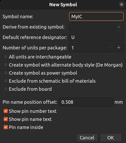
To start, create the symbol
- Open the symbol editor (in KiCad's main window)
- Select SWLib in the libraries panel on the left
- Select the new symbol button (or
File > New Symbol...) - Name the symbol. This should typically match the name of the part you are making a symbol for.
- Optionally select an existing symbol to derive from ("start with")
- Change the designator if needed. See this
- Typically, units per package should be left as 1
-
Leave other settings unchanged
-
Click OK to create you symbol. It will be open in the editor.
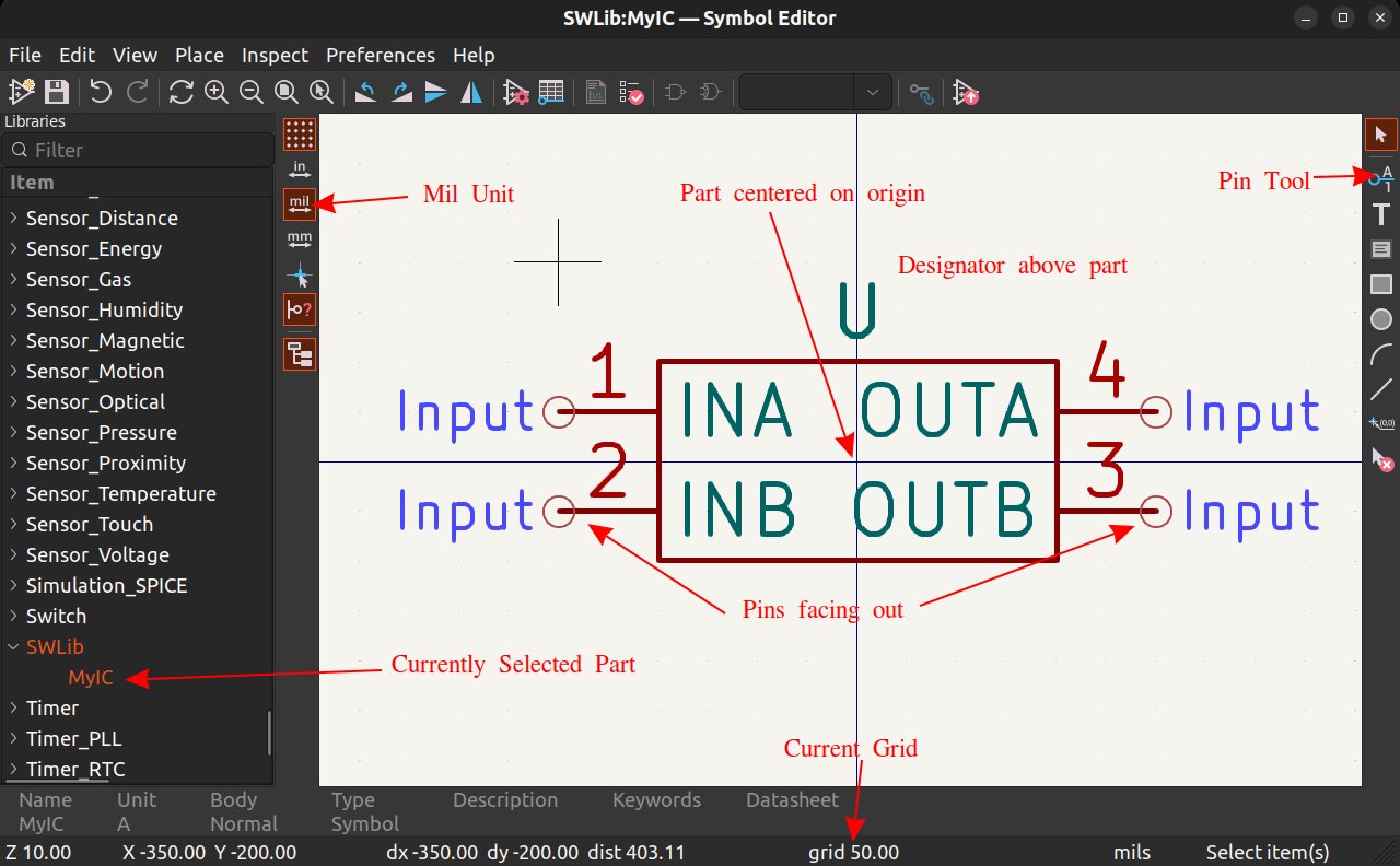
- Make sure the unit is set to "mil" on the left hand toolbar.
- Make sure the grid is set to 50mil (
View > Grid Properties). You can see the current grid on the bottom bar. - Create the symbol. You can use the tools on the right toolbar to "draw" the symbol (lines, shapes, arcs). Draw your part centered on the origin!
- Then use the "pin" tool (right toolbar) to add the required number of pins. Name the pins using the names in the part's datasheet. Make sure the pin number match the part's package pin numbers. When creating pins, the "circle" should be facing out. THis is where wires connect to in the schematic.
- Make sure to drag the designator above the part
-
Save!
After creating the symbol, determine if you need to create a footprint. KiCad's footprint libraries have a footprint for most standard packages (0603, 0805, 1206, etc for resistors, capacitors, diodes, inductors; QFP, TSSOP, SOIC, DIP, QFN, etc for ICs). Open the footprint editor and search for the package your device uses. If it exists, do not create a custom footprint. Skip to step 6. If you do need to create the footprint, follow the instructions below.
- Open the footprint editor
- Select "SWLib" in the left panel with all libraries
- Select
File > New Footprintto create an empty footprint. Name it the same as your part. - Use the footprint editor to place pads and draw any desired silkscreen. Make sure the numbers of the pads match the numbers of the pins the pad should be associated with. Follow numbering convention in the part's datasheet.
-
Save!
-
Go back to your part in the Symbol editor.
- Edit symbol properties (
File > Symbol Properties...) - Click the library icon next to the footprint field (you may need to click the footprint field first).
- Select the footprint for your part
- Double check the pin number order of the footprint and schematic. This is especially important if you are using a footprint you did not make.
- Save!
Optionally, you can add a 3D model to a footprint.
- Create or download a 3D mode. Save it as a step or stl file in
SW-KicadLibrary/SWLib.3d. Name it the same as the part. - Open the footprint editor and select your part.
- Edit footprint properties (
File > Footprint Properties...) - Select the 3D models tab
- Click the plus button and type the following. Never use the browse feature to select a 3d model! Browse tool uses absolute paths, which will break the model on other people's systems.
../../SWLib.3d/[FILE].step - Replace
[FILE]with the name of the step file. This is case sensitive!. - Close the properties panel and save the footprint.
After creating your part (and saving everything) commit your changes in the SW-KicadLibrary repo and push.
Importing Downloaded Parts
Many parts will have footprints and symbols (ECAD models) available for download. These often include 3D models too. Some common sources to find these models are
- SamacSys (easiest to access through mosuer; DO NOT INSTALL THE LIBRARY LOADER! DO NOT USE IT!)
- UltraLibrarian
- SnapEDA
Note that you will need an account to use any of these services.
- When downloading a model, download symbol and footprint. If a 3D model is available, download it too.
-
After downloading, follow the instructions below depending on where you downloaded the model from. Note that if a 3D model was not available, the 3D model file will be missing.
SamacSys
The downloaded file will be a
.zipfile. Extract it.Locate the following three files.- Symbol:
[PART]/KiCad/[PART].kicad_sym(older parts may only have a.libfile. This works too.) - Footprint:
[PART]/KiCad/[PACKAGE].kicad_mod - 3D Model:
[PART]/3D/[PART].stp
UltraLibrarian
The downloaded file will be a
.zipfile. Extract it.Locate the following three files.- Symbol:
KiCAD/[NAME]/[NAME].lib - Footprint:
KiCAD/[NAME]/footprints.pretty/[NAME].kicad_mod - 3D Model:
[NAME]/STEP/[NAME].step
SnapEDA
The downloaded file will be a
.zipfile. Extract it.Locate the following three files.- Symbol:
[PART].kicad_sym - Footprint:
[PART].kicad_mod - 3D Model:
[PART].step
- Symbol:
-
Open KiCad's symbol editor
- Find SWLib in the panel on the left.
- Right click "SWLib" and choose "Import Symbol..."
- Choose the symbol file (
.lib) described above. - Save the symbol.
- Open the footprint editor.
- Find SWLib in the panel on the left.
- Right click "SWLib" and choose "Import Footprint..."
- Choose the footprint file (
.kicad_mod) described above. - Save into SWLib
- Copy the 3D model file (
.step/.stpfile described above) to SWLib. This must be copied to wherever you cloned SWLib. Paste the.stepfile intoSW-KicadLibrary/SWLib.3d - In the footprint editor, edit footprint properties (
File > Footprint Properties...) - Select the 3D models tab
- Click the plus button and type the following. Never use the browse feature to select a 3d model! Browse tool uses absolute paths, which will break the model on other people's systems.
../../SWLib.3d/[FILE].step - Replace
[FILE]with the name of the step file. This is case sensitive!. Changestepto a different suffix if the file uses a different suffix. - Close the properties panel and save the footprint.
- Go back to the symbol editor and select the imported symbol.
- Open symbol properties (
File > Symbol Properties...) - Click the footprint field, then select the browse button
- Choose the footprint now imported into the SWLib footprint library
- Close the symbol properties panel and save.
After importing your part (and saving everything) commit your changes in the SW-KicadLibrary repo and push.
Creating a New Project
Make sure you have installed SWLib first!
TODO
Opening an Existing Project
Make sure you have installed SWLib first!
TODO
Design Workflow
Schematic
Always use a 50mil grid in the schematic editor! If absolutely necessary, a 25mil grid can be used occasionally, but try to avoid doing so.
TODO: General schematic work
TODO: Symbol table conventions and custom part number field
TODO: Net label and power port behavior across multiple schematic sheets
Electrical Rules Check
TODO
Assign footprints
TODO (note bulk procedures too)
PCB Setup
It is generally necessary to setup some board stackup parameters (specifically the number of copper layers) before starting the PCB. In order to make running DRCs later, it is best to import board settings from one of the SW-KiCadTemplates. These templates are based on PCB manufacturer board stackups and include design rules. Specifics (such as board color, default item sizes, etc) can be customized after importing a template. To import a template, follow the steps listed below
- Download a zip of the repo and extract the zip (or just clone it)
- Open your project in KiCad
- Open your PCB
- Open Board Setup (
File > Board Setup) - Click the button on the bottom left labeled "Import Settings from Another Board"
- Choose the
kicad_pcbfile for the template you want to use. Which template is used should depend on how you plan to design the PCB (number of layers, impedance control, etc) as well as who you plan to have manufacture the PCB. - After selecting a template file, click the "Select All" button (rarely will you want to import only some settings)
- Click "Import Settings"
- Click "OK" to close the board setup dialog
- Save the PCB file
- Restart KiCad (Close fully and reopen the project). Skipping this step can cause library issues until KiCad is restarted.
PCB Layout & Routing
Always work in mil not mm grid!
TODO
Design Rules Check (DRC)
- Setup design rules in Boards Setup (
File > Board Setup). Fill in options forDesign Rules > Constraintsand change defaults inText & Graphics > Defaultsas applicable. Skip this if you imported board settings from one of the template boards! Close Board Setup dialog when done. - Open the design rules checker dialog (
Inspect > Design Rules Checker) - At the top, select only "Refill all zones before performing DRC"
- Make sure both errors and warnings are shown (checkboxes near bottom of the dialog)
- Run the DRC
- Fix any errors.
- Fix or waive warnings as warranted.
Tips and Tricks
Flat multi-page Schematics
There are two common ways of doing multi-page schematics: Hierarchical and flat. Hierarchical design embeds one sheet as a block in another. Connections between sheets are made using ports. Flat designs have multiple sheets (all considered top level). Connections between sheets are made by naming nets the same name. AquaPack prefers to use Hierarchical design over flat design practices.
In rare cases it may be acceptable to use a flat design, however KiCad doesn't really support them well. You still have to create a top level schematic and add all your sheets as blocks to it. However you just won't add ports or make connections. The top level sheet just acts as a container.
HandSolder Footprints
The builtin KiCad footprint libraries often have two variants of footprints (eg for resistors, capacitors, etc). One is often suffixed "HandSolder". These footprints use elongated pads that make it easier to solder components to the board by hand. These are generally preferred for our use cases.
Mounting Holes
Do not use vias or manually placed pads for mounting holes. This will lead to DRC warnings / errors. Instead use footprints from the builtin "MountingHole" library. These footprints can be added to the PCB without corresponding symbols in the schematic by using the "Add Footprint" option in the PCB editor (Place > Add Footprint). After adding the footprint, make sure to edit its properties and check the "Not in schematic" box.
Silkscreen Text size
Most manufacturers specify limits on character height and stroke width. KiCad also wants a character width. Always make this equal the the height of your characters!
Adding Images to Silkscreen
- Open the project you want to add images to
- In KiCad's project window open the "Image Converter"
- Click Load Image and choose the image you want to add. Monochrome bitmaps work well. Other image formats work, but you may need to adjust the black / white threshold.
- Choose the size of the image in "Output Size" (if not sure what size you want guess; trial and error is the way to go)
- Choose "Footprint (.kicad_mod file)" for Output Format
- Make sure "Front Silkscreen" is selected for the layer
- Click "Export to Clipboard" (there is generally no reason to save graphics as symbol files)
- Open the PCB (it is recommended to still leave the image converter window open for now too)
- Paste the symbol (Ctrl+V for normal people or CMD+V on mac) and place it where you want on the board
- To place on the back of the board, press the F key with the graphic selected.
- If the size is wrong, do not attempt to resize it in the PCB. Go back to the image converter window, change the size and export to clipboard again. Paste it into the PCB again. Repeat as needed.
- Once the graphic is paced where you want it, double click it to open its properties (footprint properties) and uncheck the "Show" box next to "Reference Designator". Click OK to close the dialog.
- Note that when you run the DRC check, there will be a footprint warning about the graphic. Just exclude the violation.
Thermal Relief Connections to Pads
When connecting a zone to a pad, it will be thermally relieved by default. This means it will be connected with "spokes" instead of solid copper. This is usually desirable, however it can be disabled in the properties of the zone if you need to or specific cases (usually only necessary for high current or if using copper on the board as a heatsink).
Other Useful Options / Features of PCB Editor
- You can fill or unfill all copper zones (sometimes called "polygons" or "pours" or "planes") by using
Edit > Fill All ZonesandEdit > Unfill All Zones. Unfilling zones is useful while working on the board. Filling them lets you see how the zone will be filled after updating the zone itself. - You can flip the board view using
View > Flip Board View. This is sometimes useful if working on the back of the board. This pairs well with the layer presets on the right below the layer selector (for example, select the all back layers preset). - When editing tracks (traces) you can select one part and use the "U" and "I" keys to select more or less of the track.
- You can bulk edit fonts of silkscreen text using
Edit > Edit Text and Graphics Properties.... - You can automatically cleanup traces and vias (remove redundant segments, etc) using
Tools > Cleanup Tracks and Vias.... However, be careful with the "Delete redundant vias" option. This may delete vias you wanted multiple of for current or heat reasons.